

Home / Products / Integrated circuits / Logic ICs /
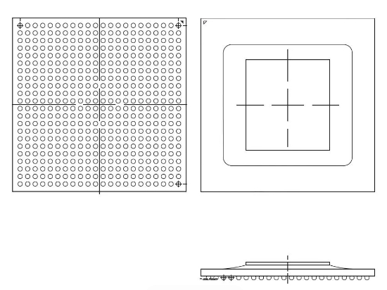

XC7A200T-2FBG484I
| Manufacturer Part Number: XC7A200T-2FBG484I | Manufacturer / Brand: Xilinx |
| Part of Description: FPGA - Field Programmable Gate Array XC7A200T-2FBG484I | Lead Free Status / RoHS Status:  Lead free / RoHS Compliant Lead free / RoHS Compliant |
| Ship From: HK/Shen Zhen | Shipment Way: DHL/Fedex/TNT/UPS |
| Datasheets: |
Product parameters
| Manufacturer | Xilinx |
| RoHS | Details |
| Mounting Style | SMD/SMT |
| Package / Case | FCBGA-484 |
| Embedded Memory | 12.83 Mbit |
| Number of Logic Elements | 215360 LE |
| Number of I/Os | 285 I/O |
| Minimum Operating Temperature | – 40 C |
| Maximum Operating Temperature | + 85 C |
| Packaging | Reel |
| Factory Pack Quantity | 60 |
| Subcategory | Programmable Logic ICs |
| Tradename | Artix |
| Unit Weight | 0.857060 oz |
Get in touch with us now
Related Products
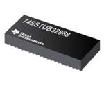
74SSTUB32868ZRHR
- Manufacturer / Brand: Texas Instruments
- Description: New original
- Ship From: HK/Shen Zhen
- Data sheet: datasheet-1667368970.pdf
Quote:
RFQ
SN74CBTLV3257D
- Manufacturer / Brand: Texas Instruments
- Description: New original
- Ship From: HK/Shen Zhen
- Data sheet: datasheet-1667368992.pdf
Quote:
RFQ
SN74LV4052AD
- Manufacturer / Brand: Texas Instruments
- Ship From: HK/Shen Zhen
- Description: New original
- Data sheet:
Quote:
RFQ
THS6222IRHFR
- Manufacturer / Brand: Texas Instruments
- Description: New original
- Ship From: HK/Shen Zhen
- Data sheet: datasheet-1667368952.pdf
Quote:
RFQ
SN74CB3Q3257PW
- Manufacturer / Brand: Texas Instruments
- Ship From: HK/Shen Zhen
- Description: New original
- Data sheet: datasheet-1676970581.pdf
Quote:
RFQ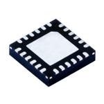
THS6222IRHFT
- Manufacturer / Brand: Texas Instruments
- Description: New original
- Ship From: HK/Shen Zhen
- Data sheet: datasheet-1667368958.pdf
Quote:
RFQ
TS5A3166DBVRG4
- Manufacturer / Brand: Texas Instruments
- Ship From: HK/Shen Zhen
- Description: New original
- Data sheet:
Quote:
RFQ
TS3A5018D
- Manufacturer / Brand: Texas Instruments
- Ship From: HK/Shen Zhen
- Description: New original
- Data sheet:
Quote:
RFQ
