

Home / Products / Integrated circuits / Logic ICs /
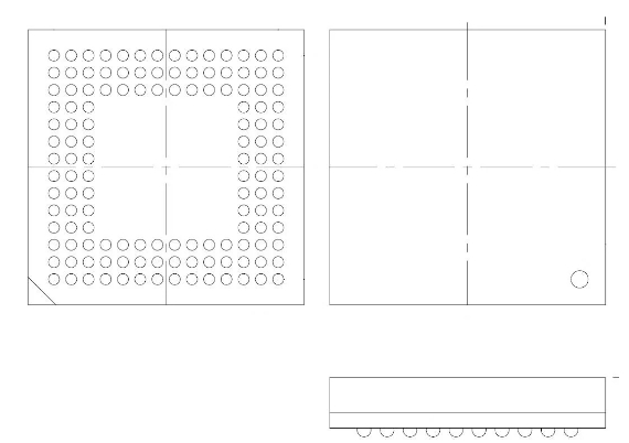

XC3S250E-4CPG132C
| Manufacturer Part Number: XC3S250E-4CPG132C | Manufacturer / Brand: Xilinx |
| Part of Description: FPGA - Field Programmable Gate Array XC3S250E-4CPG132C | Lead Free Status / RoHS Status:  Lead free / RoHS Compliant Lead free / RoHS Compliant |
| Ship From: HK/Shen Zhen | Shipment Way: DHL/Fedex/TNT/UPS |
| Datasheets: |
Product parameters
| Manufacturer | Xilinx |
| RoHS | Details |
| Mounting Style | SMD/SMT |
| Package / Case | CSBGA-132 |
| Distributed RAM | 38 kbit |
| Embedded Block RAM – EBR | 216 kbit |
| Maximum Operating Frequency | 300 MHz |
| Minimum Operating Temperature | – 40 C |
| Maximum Operating Temperature | + 85 C |
| Factory Pack Quantity | 360 |
| Subcategory | Programmable Logic ICs |
| Tradename | Spartan |
| Unit Weight | 0.112800 oz |
Get in touch with us now
Related Products
74LVC1G3157DBVRG4
- Manufacturer / Brand: Texas Instruments
- Ship From: HK/Shen Zhen
- Description: New original
- Data sheet: datasheet-1676970595.pdf
Quote:
RFQ
SN74LV4052AD
- Manufacturer / Brand: Texas Instruments
- Ship From: HK/Shen Zhen
- Description: New original
- Data sheet:
Quote:
RFQ
SN74LV4052AD
- Manufacturer / Brand: Texas Instruments
- Ship From: HK/Shen Zhen
- Description: New original
- Data sheet:
Quote:
RFQ
SN74LV4052APW
- Manufacturer / Brand: Texas Instruments
- Ship From: HK/Shen Zhen
- Description: New original
- Data sheet:
Quote:
RFQ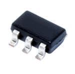
TS5A3166DBVRG4
- Manufacturer / Brand: Texas Instruments
- Ship From: HK/Shen Zhen
- Description: New original
- Data sheet:
Quote:
RFQ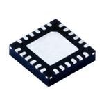
THS6222IRHFR
- Manufacturer / Brand: Texas Instruments
- Description: New original
- Ship From: HK/Shen Zhen
- Data sheet: datasheet-1667368952.pdf
Quote:
RFQ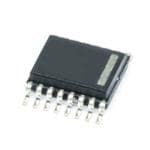
SN74CBTLV3257DBQR
- Manufacturer / Brand: Texas Instruments
- Description: New original
- Ship From: HK/Shen Zhen
- Data sheet: datasheet-1667368998.pdf
Quote:
RFQ
74CBTLV3257PWRG4
- Manufacturer / Brand: Texas Instruments
- Description: New original
- Ship From: HK/Shen Zhen
- Data sheet: datasheet-1667368986.pdf
Quote:
RFQ
