

Home / Products / Integrated circuits / Logic ICs /

CD4049BE
| Manufacturer Part Number: CD4049BE | Manufacturer / Brand: XBLW |
| Part of Description: The CD4049BE is a hex buffer/inverter CMOS integrated circuit that provides six independent buffers/inverters in a single package. Each buffer/inverter can be configured as either a buffer or an inverter | Lead Free Status / RoHS Status: Digital Signal Processors & Controllers - DSP, DSC 16 BIT HYBRID CNTRLR |
| Ship From: HK/Shen Zhen | Shipment Way: DHL/Fedex/TNT/UPS |
|
Datasheets:
|
Product parameters
| Manufacturer | XBLW |
| Details | RoHS |
| Mounting Style | SMD/SMT |
| Package / Case | DIP-14 |
| Supply Voltage – Min | – 40 C |
| Supply Voltage – Max | +85 C |
| Packaging | Tube |
| Moisture Sensitive | Yes |
| Factory Pack Quantity | 100 |
Get in touch with us now
Related Products

SN74LV4051AD
- Manufacturer / Brand: Texas Instruments
- Ship From: HK/Shen Zhen
- Description: New original
- Data sheet:
Quote:
RFQ
SN74LV4052AD
- Manufacturer / Brand: Texas Instruments
- Ship From: HK/Shen Zhen
- Description: New original
- Data sheet:
Quote:
RFQ
SN74CBTLV3257DBQR
- Manufacturer / Brand: Texas Instruments
- Description: New original
- Ship From: HK/Shen Zhen
- Data sheet: datasheet-1667368998.pdf
Quote:
RFQ
SN74LV4052AN
- Manufacturer / Brand: Texas Instruments
- Ship From: HK/Shen Zhen
- Description: New original
- Data sheet: datasheet-1677218988.pdf
Quote:
RFQ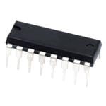
CD74HC4051E
- Manufacturer / Brand: Texas Instruments
- Ship From: HK/Shen Zhen
- Description: New original
- Data sheet:
Quote:
RFQ
TS3A5018D
- Manufacturer / Brand: Texas Instruments
- Ship From: HK/Shen Zhen
- Description: New original
- Data sheet:
Quote:
RFQ
74SSTUB32868AZRHR
- Manufacturer / Brand: Texas Instruments
- Description: New original
- Ship From: HK/Shen Zhen
- Data sheet: datasheet-1667368980.pdf
Quote:
RFQ
TS3A5018PW
- Manufacturer / Brand: Texas Instruments
- Ship From: HK/Shen Zhen
- Description: New original
- Data sheet:
Quote:
RFQThe CD4049BE is a monolithic complementary metal-oxide-semiconductor (CMOS) integrated circuit that functions as a hex buffer/inverter. It provides six independent buffers/inverters in a single package, allowing for versatile use in various digital logic applications.
Each of the six buffers/inverters in the CD4049BE can be configured to either pass the input signal through as a buffer or invert the input signal as an inverter. This flexibility makes the CD4049BE a highly useful component in circuits that require both buffering and inverting capabilities.
The CD4049BE operates with a wide supply voltage range, typically between 3V and 15V, making it suitable for use in both low-voltage and high-voltage applications. Its CMOS technology ensures low power consumption and high noise immunity, contributing to reliable operation in demanding environments.
The IC features high source and sink current capability, allowing it to drive multiple loads effectively. Additionally, it offers special input protection that permits input voltages greater than the supply voltage, providing added safety and stability in circuits.
The CD4049BE is packaged in a dual-in-line package (DIP) or other surface-mount packages, depending on the specific version, with 16 pins for easy integration into existing circuits. Its compact size and pinout configuration make it an ideal choice for designers looking to optimize space and simplify circuit layout.
In terms of applications, the CD4049BE can be used as a hex buffer, a CMOS to DTL/TTL converter, or as a CMOS current driver. It is particularly useful in circuits that require logic level conversion, such as those interfacing CMOS with DTL or TTL logic families.
Overall, the CD4049BE is a versatile and reliable CMOS integrated circuit that offers six independent buffers/inverters in a single package. Its wide supply voltage range, low power consumption, high noise immunity, and compact packaging make it an ideal choice for a wide range of digital logic applications.
Please note that this description is based on general information about the CD4049BE and may not cover all specific details or variations of the product. For more detailed information, please refer to the official datasheet provided by the manufacturer.

