

Home / Products / Integrated circuits / Logic ICs /
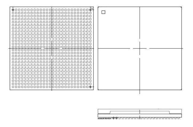

XC7K160T-2FFG676I
| Manufacturer Part Number: XC7K160T-2FFG676I | Manufacturer / Brand: Xilinx |
| Part of Description: FPGA - Field Programmable Gate Array XC7K160T-2FFG676I | Lead Free Status / RoHS Status: Digital to Analog Converters - DAC Dual, 16-Bit, 1230 MSPS, TxDAC+ Digital-to-Analog Converter |
| Ship From: HK/Shen Zhen | Shipment Way: DHL/Fedex/TNT/UPS |
| Datasheets: |
Product parameters
| Manufacturer | Xilinx |
| Details | RoHS |
| Mounting Style | SMD/SMT |
| Package / Case | FCBGA-676 |
| Minimum Operating Temperature | – 40 C |
| Maximum Operating Temperature | +100 C |
| Embedded Block RAM – EBR | 11700 kbit |
| Moisture Sensitive | Yes |
| Product Type | FPGA – Field Programmable Gate Array |
| Factory Pack Quantity | 40 |
| Subcategory | Programmable Logic ICs |
| Operating Supply Voltage | 1.2 V to 3.3 V |
| Tradename | Kintex |
| Unit Weight | 3.506996 oz |
Get in touch with us now
Related Products
THS6222IRHFT
- Manufacturer / Brand: Texas Instruments
- Description: New original
- Ship From: HK/Shen Zhen
- Data sheet: datasheet-1667368958.pdf
Quote:
RFQ
SN74CB3T3245PW
- Manufacturer / Brand: Texas Instruments
- Ship From: HK/Shen Zhen
- Description: New original
- Data sheet:
Quote:
RFQ
74CBTLV3257PWRG4
- Manufacturer / Brand: Texas Instruments
- Description: New original
- Ship From: HK/Shen Zhen
- Data sheet: datasheet-1667368986.pdf
Quote:
RFQ
SN74LV4051AD
- Manufacturer / Brand: Texas Instruments
- Ship From: HK/Shen Zhen
- Description: New original
- Data sheet:
Quote:
RFQ
SN74LV4052AN
- Manufacturer / Brand: Texas Instruments
- Ship From: HK/Shen Zhen
- Description: New original
- Data sheet: datasheet-1677218988.pdf
Quote:
RFQ
SN74CBTLV3257D
- Manufacturer / Brand: Texas Instruments
- Description: New original
- Ship From: HK/Shen Zhen
- Data sheet: datasheet-1667368992.pdf
Quote:
RFQ
74LVC1G3157DBVRG4
- Manufacturer / Brand: Texas Instruments
- Ship From: HK/Shen Zhen
- Description: New original
- Data sheet: datasheet-1676970595.pdf
Quote:
RFQ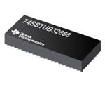
74SSTUB32868ZRHR
- Manufacturer / Brand: Texas Instruments
- Description: New original
- Ship From: HK/Shen Zhen
- Data sheet: datasheet-1667368970.pdf
Quote:
RFQThe XC7K160T-2FFG676I is a state-of-the-art Field-Programmable Gate Array (FPGA) chip produced by Xilinx, belonging to the Kintex-7 series. This chip is designed to provide exceptional performance and power efficiency, making it ideal for a wide range of applications.
Key Features and Specifications:
- Advanced Process Technology:
- Manufactured using a 28-nanometer High-K Metal Gate (HKMG) High Performance Logic (HPL) process.
- Offers options for 1.0V or 0.9V core voltage, enabling low power consumption.
- High-Performance Logic:
- Contains a large number of programmable logic units (LUTs), ranging from approximately 159,200 to 162,240, depending on specific configurations.
- Supports complex digital logic functions and high-speed data processing.
- Block RAM (BRAM):
- Features a significant amount of BRAM capacity, up to 34Mb, for efficient data storage and access.
- Supports high-speed data buffering and processing needs.
- Input/Output (I/O) Capabilities:
- Offers 250 input/output pins, with support for differential signaling and multiple standard interface protocols such as PCI Express, SATA, and USB.
- Provides flexibility for connecting to various external devices and systems.
- Clock Management:
- Incorporates advanced clock management tiles (CMTs) with PLL (Phase-Locked Loop) and MMCM (Mixed-Mode Clock Manager) modules.
- Enables high-precision and low-jitter clock signaling, critical for high-speed data processing and communication.
- DSP Slices:
- Equipped with DSP slices, including multipliers and accumulators, for high-performance digital signal processing tasks.
- Supports applications such as signal processing, image processing, and more.
- Packaging:
- Available in a 676-pin Fine-Pitch Ball Grid Array (FBGA) package, with options for low-cost, high-signal integrity packaging.
- Supports industrial-grade temperature ranges from -40°C to +100°C, suitable for harsh environments.
- High-Speed Interfaces:
- Supports high-speed serial interfaces, including Gigabit Ethernet, XAUI, and other high-speed protocols.
- Enables high-bandwidth data transmission and communication.
- Design and Programming Flexibility:
- Supports VHDL and Verilog, two mainstream hardware description languages, allowing users to program and design according to their specific needs.
- Offers dynamic reconfiguration capabilities, enabling users to reconfigure parts of the logic during runtime for higher flexibility and reliability.
- Rich IP Cores and Peripheral Interfaces:
- Provides a rich library of IP cores, including DSP, memory, and interface cores, facilitating rapid system development.
- Equipped with various peripheral interfaces such as Ethernet, USB, and storage interfaces for high-speed communication and data exchange with other devices.
Applications:
The XC7K160T-2FFG676I is suitable for a variety of applications, including but not limited to:
- Communications: Used in high-speed data transmission, protocol conversion, and baseband processing in communication infrastructure.
- Video and Image Processing: Enables high-definition video encoding, decoding, and image analysis, widely used in video and image processing fields.
- Industrial Automation: Applied in control logic, motion control, and sensor interfaces in industrial automation to improve production efficiency and product quality.
- Medical Equipment: Supports digital signal processing and control system design for medical equipment, such as medical imaging and biological signal processing.
- Aerospace and Defense: Plays a crucial role in aerospace control and navigation systems, providing high reliability and stability solutions.
In summary, the XC7K160T-2FFG676I is a high-performance, high-integration, and flexible programmable FPGA chip. Its advanced process technology, rich features, and wide range of applications make it an ideal choice for various fields.

